


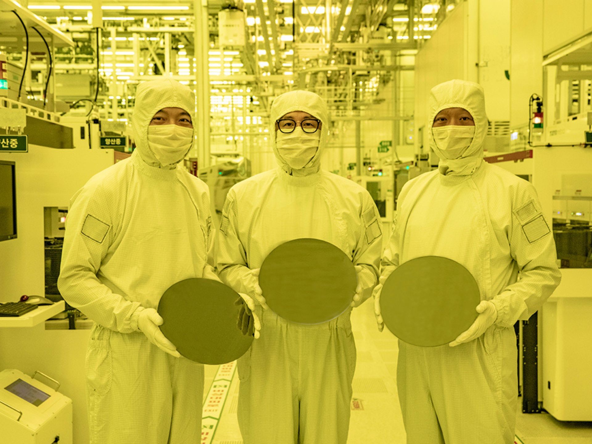
(From left) Michael Jeong, Company Vice President; Ja-Hum Ku, Company Government Vice President; and Sang Bom Kang, Company Vice President at Samsung Foundry Enterprise are holding up 3nm wafers on the manufacturing line of Samsung Electronics Hwaseong : Samsung
Everyone knows that Samsung makes among the finest smartphones in the marketplace, however many customers typically desire the Qualcomm chips over the Exynos variants as they’re extra highly effective and environment friendly. That, nonetheless, doesn’t cease Samsung from innovating and dealing on new fabrication processes, and it developed a brand new 3nm know-how, paving the way in which for brand new extra highly effective, and extra environment friendly chips to be manufactured at its amenities.
Samsung Foundry introduced its starting mass manufacturing of first-generation chips, based mostly on the 3nm know-how. The brand new chips can be based mostly on the brand new Gate-All-Round (GAA) transistor structure, changing the earlier FinFET. The brand new 3nm know-how will supply important enhancements in comparison with the 5nm know-how, specifically a 23% efficiency replace, and the chip can be as much as 45% extra power-efficient. The chip can also be 16% smaller.
“Optimized 3nm course of achieves 45% diminished energy utilization, 23% improved efficiency and 16% smaller floor space in comparison with 5nm course of”
The primary-generation 3nm chips will initially be accessible for high-performance, low-power computing gadgets, however Samsung plans to develop it to cellular processors in the longer term. We sit up for seeing how this develops over the approaching months and years, and we’re excited to see the doorways this new know-how opens for smartphones, tablets, and computer systems.
How does it work?
: Samsung
Samsung explains that the brand new proprietary know-how makes use of nanosheets with wider channels, permitting for increased efficiency and larger power effectivity in comparison with GAA applied sciences utilizing nanowires with narrower channels. The brand new 3nm GAA know-how will permit Samsung to regulate the width of the nanosheet to optimize the facility utilization and efficiency, rising the facility output and considerably bettering the effectivity.
The corporate additionally stated that the brand new GAA structure affords extra design flexibility, permitting for larger advantages for optimizing the facility and boosting efficiency. The second-generation 3nm course of is predicted to scale back the facility consumption by as much as 50% whereas bettering the efficiency by 30% in a 35% smaller space. These outcomes are spectacular, and seem like higher than the annual upgrades we see in chipsets, though the real-world use will probably differ based mostly on the working system and the aim they’re used for.
What are the advantages?
: Samsung
As talked about above, Samsung claims to attain 45% diminished energy utilization, 23% improved efficiency on a 16% smaller floor space, in comparison with the 5nm course of. These numbers recommend that real-world functions will profit significantly from the brand new structure and the brand new course of, proving to be higher for all types of functions.
Smartphones, computer systems, tablets, and different gadgets will profit from the brand new know-how as they’ll be capable to pack extra energy in a smaller space. As the facility will increase, the effectivity may also develop increased, making the gadgets last more, whereas consuming much less energy. The performance of those chips may also develop into extra in depth, and OEMs will be capable to supply extra {hardware} and software program options consequently.
Present high-end smartphones have 4nm processors, such because the Qualcomm Snapdragon eight Gen 1 SoC. These chips are already highly effective and environment friendly, however there’s at all times room for enchancment. Semiconductor factories, reminiscent of TSMC, are additionally engaged on delivering 3nm chips someday this 12 months, and it seems like Samsung managed to take over and announce the know-how first. TSMC, and different semiconductor corporations are additionally closely investing in 2nm fabrication processes, and they’re going to probably be accessible in the approaching years, providing even higher effectivity and efficiency.
Samsung is predicted to start the mass manufacturing of 3nm chips in the second half of 2022, and we might see new computing functions arrive with the brand new chips quickly. It’s unclear what gadgets will obtain it first, and we’re unlikely to see new gadgets geared up with such chips this 12 months.